With such a huge range of smartphone hardware on the market today from vendors such as Samsung, HTC, Apple, Motorola, LG and more, it can be very confusing to keep up with what exactly is inside each of these devices. There are at least 10 different CPUs inside smartphones, many different GPUs, a seemingly endless combination of display hardware and a huge variety of other bits and bobs.
This multi-part guide is intended to help you understand each and every one of the critical components in your smartphone and how they compare to other hardware on the market. Each section is intended to give you all the necessary information about the hardware, and even more for the tech enthusiasts out there, so expect them all to be lengthy and filled with details.
Over the next several days and weeks we’ll be posting up another part of the guide. In today’s guide I’ll be looking at smartphone processors: the different brands, types, how they perform and the critical differences between them.
- Part 1: Processors (this article)
- Part 2: Graphics
- Part 3: Memory & Storage
- Part 4: Displays
- Part 5: Connectivity & Sensors (coming soon)
- Part 6: Batteries (coming soon)
- Part 7: Cameras (coming soon)
System-on-a-Chip
This is a term you’ve probably come across before, and for good reason. When reviewers are talking about the processors inside a smartphone they are usually actually referring to the system-on-a-chip: a combination chipset that features things such as the actual processor cores, the graphics chipset, the RAM and possibly ROM as well, interface controllers for things such as USB and wireless tech, voltage regulators and more.

The idea behind a system-on-a-chip, or SoC, is that all the critical components of a device are located in a relatively small area on the device. This reduces the size of the component board needed inside and also can help make the device itself faster and more battery efficient. They also help reduce costs for assembling the product and can also be cheaper than an equivalent multi-chip set-up.
I’m more specifically looking at the processing cores inside the SoC as well as available SoC packages today, but you can look out for the other parts of this article for more detailed information on the graphics chip, memory and more.
What does ARM have to do with it?
References to ARM when it comes to SoCs can unfortunately be confusing. ARM is essentially three things: a company, a microprocessor architecture and processor core; all of which you may have guessed are related. ARM Holdings plc is the British-based company that, since 1983, has developed the ARM microprocessor instruction architecture which is used inside their ARM processor cores.
Where other companies like NVIDIA, Texas Instruments and Samsung come in is in the production of the SoCs. They take (through licensing) the ARM developed and produced processor core and put it inside their chipsets in combination with whatever GPUs, memory and other things they desire. Qualcomm is a slightly different story, but we’ll get to that later.
This is why two SoCs from different companies can both appear to contain the same processor, such as how both the TI OMAP3630 and Samsung Exynos 3310 use a single-core 1 GHz ARM Cortex-A8 solution. They are different though in their use of other components, such as how the OMAP uses a PowerVR SGX530 GPU but the Exynos features the SGX540.

The ARM1 building in Cambridge, where integral parts of smartphones are developed
The ARM architecture is something that you don’t really have to worry about when looking at a new smartphone as almost all new ARM processors feature their ARMv7 architecture. The older ARMv6 architecture was used on old ARM11 processors, which in turn were used in old SoCs on devices such as the HTC Dream (T-Mobile G1, the first Android phone) and iPhone 3G.
Currently there are two ARM processor types that are widely in use: the ARM Cortex-A8 and ARM Cortex-A9 MPCore; both use the ARMv7 architecture. Without getting extremely technical, the Cortex-A8 is usually found in single-core implementations and the Cortex-A9 in devices with up to 4 cores. The A9 is the newer implementation and as well as being (usually) multi-core, it is slightly faster per MHz than the A8 processors (2.0 DMIPS/MHz vs. 2.5 DMIPS/MHz).
You’ll find the ARM Cortex-A8 processor inside SoCs such as the TI OMAP3 series and Samsung’s SP5C series (Hummingbird/Exynos 3xxx). The Cortex-A9 is found in the TI OMAP4 series, Samsung Exynos 4xxx series, NVIDIA’s Tegra 2/3 and the Apple A5.
ARM also makes the Mali range of graphics processors, which I’ll be looking at in the graphics part of this series.
In the future we’ll be seeing SoCs that feature ARM’s Cortex-A15 MPCore, which is allegedly 40% faster than the Cortex-A9. We should see these in the TI OMAP5 series, Samsung Exynos 5xxx series and the Tegra "Wayne" series in late 2012/early 2013. In the distant future we can also expect ARM cores that use their ARMv8 architecture.
Qualcomm processors and Snapdragon SoCs
Qualcomm is slightly different to the other SoC manufacturers in that they don’t actually use the reference ARM processor core designs. Instead they take cues from the ARM Cortex-A8 and make improvements that they package into their very own Scorpion and Krait CPUs. This obviously requires more research and development than say the TI OMAP series, but is apparently slightly better for media-related operations and power efficiency compared to the standard Cortex-A8.
These processors make their way into Qualcomm’s Snapdragon range of SoCs, which are split up into different series. Each series is numbered from S1 to S4 (currently), and the higher the series the more powerful and (usually) the more recent the SoCs are. As of writing there are no products on the market that make use of Qualcomm’s S4 chipsets, but they are on their way shortly.

Snapdragon SoCs are usually named using a three-letter designation followed by four numbers. “QSD” was used on the older S1 processors, followed later by “MSM” for devices with wireless connectivity and “APQ” for those without. When it comes to the numbers, the first (eg. 8xxx) indicates the class with 7 usually meaning low range and 8 meaning mid/high end. The second number (eg. x2xx) indicates whether the device is GSM or CDMA, with 2 indicating GSM and 6 indicating CDMA. The final two numbers usually designate the performance grade of the CPU: eg. the MSM8255 is a 1 GHz S2 single-core, then up to the MSM8260 1.2 GHz S3 dual-core, and then to the future MSM8270 Krait-powered S4 Snapdragon.
Both S1 and S2 Snapdragon SoCs are single-core only, ranging up to 1.5 GHz via their Scorpion processors inside. S1 was the primary and only processor type allowed in the first batch of Windows Phones, using the 1 GHz QSD8x50, and was also used in some Android devices such as the HTC Desire, HTC Droid Incredible, Nexus One and HTC EVO 4G.
The S2 Snapdragons are used in a much wider range of products. S2 differs from S1 in that there is a more powerful graphics processor inside along with a decrease in process from 65nm to 45nm, which helps conserve power and heat output allowing for larger CPU clocks. You’ll see the 1 GHz MSM8x55 in a huge range of Android products such as the HTC Desire HD, HTC Desire S, HTC Thunderbolt and pretty much all of Sony Ericsson’s first-batch of Xperia devices (including the Xperia Play).

There is also a faster S2 SoC which is the MSM8x55T which is clocked between 1.4 and 1.5 GHz. This is seen in a lot of the second generation Windows Phones such as the Nokia Lumia series, HTC Titan and Samsung Focus S. It is also used in a few Android devices such as the HTC Flyer and Samsung Galaxy W.
The S3 Snapdragons see a jump from single-core to dual-core SoCs, as well as a graphics boost. These devices are manufactured using the 45nm process and the Scorpion cores used are still Cortex-A8-based, as opposed to other dual-core SoCs that use newer Cortex-A9 technology. You’ll find the 1.2-1.5 GHz S3 MSM8x60 in products like the HTC Sensation, HTC EVO 3D, HTC Rezound and some Samsung Galaxy S II models.
Apart from the obvious differences in each series’ processor and graphics chips, along with progressively smaller manufacturing processes, each series improves on other capabilities such as camera resolution, screen resolution and media tasks. Below is a quick rundown of each series in these respects.
- Snapdragon S1: Supports up to 720p displays, 720p playback and 720p video recording. Supports up to 12 megapixel cameras. Supports up to HSPA radios
- Snapdragon S2: Improves on S2 by adding support for HSPA+. Better graphics hardware
- Snapdragon S3: Supports WSXGA (1440x900) displays, 1080p playback and 1080p recording. Supports full stereoscopic 3D capabilities including dual-cameras, recording and playback. Supports up to 16 MP cameras. Adds Dolby 5.1 surround sound support and echo/noise cancellation
Of course devices that choose to use a certain Snapdragon SoC may not choose to fully utilize the maximum capabilities of the chipset, and in fact most don’t.

A chip block diagram for the Snapdragon S4 SoCs using Krait CPUs
The next step for the Snapdragon line is the S4 series, which ditches the Scorpion CPU in favour for Qualcomm’s new Krait CPU. Krait allows for up to four cores in the SoC at up to 2.5 GHz per core, and is made on their new 28nm process. S4 also improves greatly on the GPU inside and memory capabilities, includes LTE support in the SoC, 1080p display and HDMI support, up to three 20 MP cameras, up to four microphones for recording/noise cancellation, Dolby 7.1 surround sound support, dual-band WiFi support and Bluetooh 4.0 capabilities. Qualcomm also claims that the CPU is less power hungry, which I’m guessing is mostly down to the decrease in manufacturing process size.
We should be seeing new devices with the Snapdragon S4 chipsets inside sometime this year, first announced in the Lenovo IdeaTab S2 10-inch tablet. The IdeaTab S2 should have a 1.5 GHz dual-core S4 Snapdragon 8x60A inside.
Until then, a good idea of how Qualcomm’s top-end Snapdragon S3 SoC performs can be seen in our HTC Sensation review, and from personal experience with the device it performs very well. I eagerly await testing a device with Krait inside though to see how it matches up not only to the older Snapdragons but to other SoC offerings.
Texas Instruments’ OMAP SoCs
While Qualcomm SoCs seem to be the most popular amongst smartphone manufacturers (particularly HTC), Texas Instruments’ line of OMAP (Open Media Applications Platform) systems-on-chips are also widely used. Motorola is a big fan of the TI OMAP range, and almost exclusively uses them in their Android products.
Like Qualcomm’s Snapdragon, TI OMAP SoCs come in a variety of ranges. The OMAP 1 and 2 series are quite old and you won’t find them in any new products, so it’s series 3 and 4 that we need to be concerned with in new products. Like the Snapdragon S4 products, the OMAP 5 series is the bleeding edge in TI’s range and has yet to make it into any devices.
Naming of the OMAP series is fairly straightforward, with a higher number SoC indicating better performance. The first digit is always indicative of the series, and newer series are always faster than the products in the older series. Using this logic, an OMAP4430 is better than an OMAP3630, which in turn is better than the OMAP3430.

A chip block diagram of the OMAP36xx SoCs. Note how many needed components are external
The TI OMAP 3 series is entirely single-core SoCs featuring an ARM Cortex-A8 processing core clocked between 600 MHz and 1 GHz, and the GPU inside is the PowerVR SGX530 which I’ll look at more closely in the graphics hardware article. The OMAP34xx and OMAP35xx products are both manufactured using a 65nm process, and the OMAP36xx’s using 45nm. Products using the older OMAP34xx SoCs include the Motorola Droid and Palm Pre, while the newer 36xx’s are featured inside the Motorola Defy, Motorola Droid X, Palm Pre 2, Nook Color and Nokia N9 to name a few.
The TI OMAP 4 series bumps up the specifications to dual-core ARM Cortex-A9 processors clocked between 1 and 1.8 GHz and PowerVR SGX54x GPUs. There are three products in the OMAP 4 series so far:
- The OMAP4430 used in the LG Optimus 3D and Motorola Droid Razr/Bionic (to name a few). This SoC is either clocked at 1.0 or 1.2 GHz and features the PowerVR SGX540 at 304 MHz
- The OMAP4460 is an upgraded 4430 that is clocked between 1.2 and 1.5 GHz and bumps the GPU up to 384 MHz. It’s used in the Galaxy Nexus
- The OMAP4470 can go right up to 1.8 GHz and features a considerably more powerful GPU. This SoC hasn’t been used in any products so far.
One main disadvantage to the TI OMAP line of SoCs is that the wireless radios and several other key components are not included within the chipset like they are in the Snapdragon SoCs. While this adds flexibility to add whatever communication technology you like, such as LTE, with ease, it can increase the size of the PCB needed inside the device.
However, the TI OMAP SoCs do include some other key features. TI includes their proprietary SmartReflex power-saving technology in their OMAP line, which they claim (for the OMAP 4) provides 10+ hours of 1080p playback and 120 hours of audio playback. They didn’t specify which battery they were using and what system, so take it with a grain of salt, but it sounds promising.

A chip block diagram for the TI OMAP4470
TI also has the IVA 2/3 multimedia accelerator included on the SoC die separate from the Cortex-A8/9 cores, which deals with up to 1080p media encoding and decoding on the fly. This handy addition relieves stress from the Cortex cores and as far as I can tell from Samsung's documentation their processors do not include this feature.
Another benefit of specifically the OMAP 4 series is they include two extra ARM Cortex-M3 cores which are used in low intensity situations to conserve power and save battery life. ARM’s MPE is also included that allows the SoC to run NEON code, something that NVIDIA’s Tegra range lacks; however at this stage the advantages of this are not very clear in terms of real-world performance.
The OMAP 5 series is the future of the OMAP range, and contains many features that the previous OMAP SoCs don’t have. You’ll see two ARM Cortex-A15 cores on the chip running at up to 2 GHz along with a much improved PowerVR chip, a dedicated 2D graphics chip, on-board audio processor and improved video accelerator amongst other impressive features. OMAP 5 SoCs should be starting to filter into the market in late 2012.

The Galaxy Nexus has the TI OMAP4460 SoC inside
If you’re looking at good performance benchmarks for current OMAP 4 processors, look no further than our Galaxy Nexus review that includes a performance review of the TI OMAP4460 at 1.2 GHz powering a 1280x720 display.
Samsung’s Exynos SoCs
Samsung’s Exynos range of SoCs is quite small, but fits the middle ground between a bare essentials SoC (the TI OMAP) and a fully-fledged system (the Snapdragon). When I was looking through the specifications of each SoC I was actually surprised at some of the inclusions which, for the time they were released, were ahead of the competition.

Generally speaking you will only find Samsung’s Exynos chipsets inside Samsung’s-own high-end smartphones and tablets, with one exception being the Chinese Meizu range of products. Even though Samsung do produce their own SoC, they don’t use it in all their products, often falling back to Qualcomm’s range where the Exynos chips do not meet requirements for things such as LTE and cost effectiveness.
The first of Samsung’s Exynos SoCs was known originally as the Samsung Hummingbird and resided in the original Samsung Galaxy S; it’s now known as the Samsung Exynos 3310. The Exynos 3310 was produced on a 45nm process and contains a single ARM Cortex-A8 processing core at 1.0 GHz along with a PowerVR SGX540 graphics accelerator which was very powerful for the time.
To my great surprise the original Exynos 3310 supports full 1080p encode and decode, which is something that the single-core SoCs from other companies do not support (usually maxing out at 720p). It doesn’t appear like the encoding functionality is enabled on devices like the Samsung Galaxy S and Nexus S, but according to the specifications sheet it does actually support it.
The Exynos 4210 is the second generation of the Exynos line that sees a bump to a dual-core ARM Cortex-A9 design paired with a very powerful ARM Mali-400 MP4 GPU. The SoC was originally designed to run at 1.0 GHz but was first seen at 1.2 GHz in the Samsung Galaxy S II and then 1.4 GHz in the Galaxy Note. You’ll also see the Exynos 4210 in Samsung’s Galaxy Tab 7.7.

A chip block diagram of the Exynos 4210
Not only does the dual-core Exynos 4210 improve greatly on the speed of the 3310, it also starts to include other features in the SoC. You’ll see full embedded GPS capabilities in the 4210, which is relied on by an external chip in the TI OMAP range and the Exynos 3310, and a much better modem interface that makes it easier to incorporate different radios into the system.
Like the Exynos 3310 you get full 1080p encode and decode with HDMI out in the 4210, along with USB Host capabilities. NEON code is also supported as with the TI OMAP and Snapdragon, but not NVIDIA’s Tegra 2 range. The Exynos range has no support for 3D displays/recording/decoding as far as I can tell, and there doesn’t appear to be a dedicated media accelerator so media must either be decoded fully on the GPU or CPU. Either way, it doesn’t seem to affect performance as when I used the Galaxy Note it had a huge range of supported codecs that played fine.
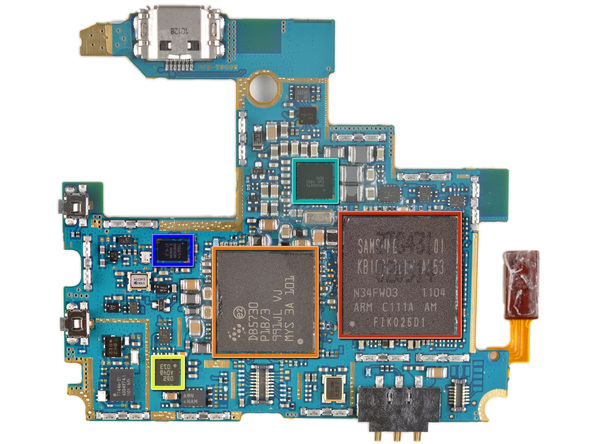
An actual Exynos processor as seen in the Samsung Galaxy S 4G (highlighted in red)
Out of the other SoCs, strangely the Exynos 4210 has the lowest maximum display resolution: 1280x800 (WXGA) vs. the Snapdragon S3’s 1440x900 (WSXGA) and the TI OMAP 4’s 1920x1200 (WUXGA). However, it can output 1080p over HDMI so it’s surprising that it can’t support 1080p interfaced displays.
The future for the Exynos chipset does look impressive though. Samsung is currently sampling the Exynos 5250, which is a 2.0 GHz dual-core ARM Cortex-A15 SoC with improved Mali graphics, stereoscopic 3D support, 2560x1600 (WQXGA) display support and much improved camera capabilities.
Benchmarks for the current Exynos 4210 SoC can be found in our Galaxy Note review which you can read here.
NVIDIA’s Tegra SoCs
Despite the fact that this SoC is indeed designed by graphics giant NVIDIA, when I look more deeply at the graphics hardware for smartphone’s you’ll discover that the Tegra line of SoCs isn’t as amazing as their desktop line of graphics cards are. It’s not to say that the SoC is bad, just that you might have been expecting a little bit more in the GPU department.
Anyway, the types of Tegra SoCs that are currently found in smartphones and tablets come from either the Tegra 2 or Tegra 3 “Kal-El” series. Both are multi-core and utilize ARM Cortex-A9 cores in their SoCs ranging from 1.0 to 1.4 GHz; both are made using a 40nm process and both use an ultra-low power (ULP) GeForce GPU as the graphics chip.
While there are similarities between the two ranges available there are some stark differences as well. For starters, the entire Tegra 2 line is dual-core whereas the Tegra 3 line is quad-core. The Tegra 3 Kal-El line uses a more powerful GPU as well, and contains some key features that the Tegra 2 SoC doesn’t have such as a companion core. However, both also can claim the feats for shipping in the first dual- and quad-core devices: the Motorola Atrix 4G and ASUS Transformer Prime respectively.
For the Tegra 2 line there are four different SoCs available: two designed for tablets and two designed for smartphones. The Tegra 250 AP20H and Tegra 250 T20 both contain 1 GHz dual-core ARM Cortex-A9 CPUs but differ in GPU clock, the faster GPU in the 250 T20 is designed for use in tablets. Then there are the 3D-capable Tegra 250 3D AP25 and Tegra 250 3D T25 which are clocked at a higher 1.2 GHz and have faster GPUs in them.
Tegra 2 SoCs lack ARM’s Advanced SIMD extension that allows the processor to execute NEON code, but as I have mentioned in the sections for other SoCs this doesn’t seem to affect a great deal. NEON allows the processor to execute MP3 playback and GSM speech at very low CPU clock cycles and also helps in the calculation of floating-point data. Again, it’s unclear what performance benefits you gain by having this capability but it mustn’t hurt to have it or NVIDIA would have left it out of Tegra 3 as well.

A look at the components of Tegra 2
According to NVIDIA’s spec sheet for the Tegra 2 SoC it seems the chipset is capable of a quite impressive range of 1080p video decoding as well as audio decoding, better than what is available on competing chips. A quick look at the block diagram reveals that, like the TI OMAP and Snapdragon SoCs, the Tegra 2 has separate processors for dealing with video and audio: in fact not just one but three.
Tegra 3 improves on Tegra 2 in many ways and beats all the competition to the first shipping quad-core SoC. Unfortunately NVIDIA had to cut corners slightly and use four Cortex-A9 cores instead of the newer Cortex-A15’s that other manufacturers are implementing in their next chipsets, but for now this shouldn’t matter.
The clock speed of these A9 cores also gets a boost from 1.2 GHz (maximum) to 1.3 GHz in a quad-core configuration, the GPU also sees a large boost and memory gets a speed and size boost as well. Tegra 3 can now also run displays that have a resolution of up to 2048x1536 (up from 1680x1050) but can still only manage two simultaneous displays where chips like the TI OMAP and Exynos can manage four and three respectively.

This is a Tegra 3 die. Notice the five cores (four full-power, one "companion") highlighted in yellow
One other cool feature of the Tegra 3 is that along with the four fully functional Cortex-A9 cores (each with NEON MPEs) there is actually a fifth Cortex-A9 “companion” core that is made using low-power transistors. The extra core runs at 500 MHz and is designed to tackle the processing of background tasks to save power, rather than having each of the four full cores run. This system is comparable to the TI OMAP 4 series’ use of Cortex-M3 cores to save power.
The future of the Tegra series lies with “Wayne”, which is said to use the newer ARM Cortex-A15 cores in either quad- or octa-core configurations. The GeForce GPU will also see a boost, but as Tegra 3 has just been launched it could be a while before we see more solid details of what this SoC will entail.
Apple SoCs
Finally we come to the last series of SoC that I’ll be looking at: Apple’s. Unlike all the others, these SoCs are not licensed and are exclusively used inside Apple’s products such as the iPhone, iPad, Apple TV and iPod Touch. As such, information about what exactly is inside these SoCs is more difficult that with the others.
Currently Apple only develops two SoCs and that’s the Apple A4 and A5 used since the iPad and iPhone 4. Before then, Apple sourced their SoCs directly from Samsung, who delivered products that eventually became the Exynos range that I have talked about previously. When the iPad came around they switched the brand name to Apple, but in fact the SoCs are still manufactured by Samsung.
The A4 is the single-core variant that includes a single ARM Cortex-A8 core clocked between 800 MHz and 1 GHz and a PowerVR SGX535 GPU. It’s made on the 45nm process and like most other SoCs it includes ARM’s MPE that allows NEON code (whatever the benefits are). It is unknown what other things may reside inside the A4, such as dedicated video hardware accelerators or ISPs, so it’s hard to tell if the A4 is more power efficient than other offerings.

The A5 jumps in with a dual-core ARM Cortex-A9 CPU and a dual-core PowerVR SGX543MP2 GPU (which is mighty fast). Most of the same things as the A4 remain such as the MPE, clock speed and 45nm process, although the A5 actually contains 512 MB of RAM unlike the A4 which used an external RAM source. There is also a dedicated image signal processor (ISP) for image post processing (most SoCs have this) as well as an “earSmart” noise cancelling unit.
Again, not much else is known about these chips and really, not much needs to be known. If you are in the market for an iPhone you have an option of these SoCs and nothing else, unlike with the Galaxy S II where you might end up with either the Exynos or Snapdragon variant.
Apple likes to keep the future of these chips tight under wraps until the next product launch, so we can only speculate as to what improvements will be made. Chances are the A6 chip will use a smaller 28nm process and include either more cores or a higher clock speed, with the possibility of using Cortex-A15 over Cortex-A9.
Which is best?
It’s really hard to say which SoC is best when you’re just looking at a few aspects of the whole package. The graphics chip makes a huge difference to the overall performance (as you’ll see in the next part in the series) and almost every chip-maker’s latest product utilizes the same ARM Cortex-A9 core at a relatively similar clock speed, and thus they have almost the same CPU performance.
Most non-graphics performance improvements come from the other components included in the SoC apart from the actual cores. For example, NVIDIA’s Tegra 2 chips lack the ARM Advanced SIMD which probably inhibits performance of the chip very slightly in media-related situations. Also, the other components in the phone that are not part of the SoC affect things, such as the size of the battery.
It’s great to see that a lot of SoC manufacturers are finding interesting ways to save power in the chipsets that they make. I was particularly interested in the addition of “companion” cores in SoC’s like the Tegra 3 (with the LP Cortex-A9 core) and the TI OMAP 4 series (with two Cortex-M3s), and as far as benchmarks go this seems to do something to help. Keep in mind though that the different set-ups of devices can greatly affect their battery life, so results from benchmarks may not indicate that the SoC is wholly responsible for great battery life.

The TI OMAP4430 SoC as seen in the Droid Razr (highlighted in light blue)
In terms of actual size the Snapdragons have a clear advantage because they manage to pack not only the processing cores, graphics chip and media accelerators in the one SoC but they also chuck in full wireless radios, GPS and RAM in the package. As this saves on other chips, the size of the PCB in theory can be cut down, leaving more internal space for batteries or slimming down the device.
There are other things that these chips can do but aren’t fully used, such as how most support camera resolutions in excess of 16 MP and display resolutions up to 1920x1200 with 1080p HDMI out as well. These are just nice numbers to know as smartphone manufacturers almost always choose parts that do not come close to maxing out the SoC’s capabilities (except the Exynos which has a relatively low supported resolution).
Personally I like the TI OMAP chips purely from the perspective that Texas Instruments seem to include many different processing chips inside the SoC that all help save power, more so than say the Exynos or Snapdragon. Although in the end, this difference is probably very minimal.
Part 2: Graphics
I hope you enjoyed this guide and learnt a bit more about what exactly is inside your smartphone and what hidden differences there are between the various SoCs. Very soon I should have up the next part of the guide which looks at smartphone graphics hardware: the other major chip that is contained within the SoC.
If you have any questions about what I have gone over in this guide please feel free to comment below or ask in our forums. I’ll try my best to answer questions but I’m not a hardware manufacturer so I might not have all the answers.
Images courtesy of Wikipedia, Qualcomm, TI, NVIDIA, Samsung, Apple, Anandtech and iFixit


24 Comments
Load the comments and join the conversation!
Read the comments, ask the editors questions, show respect and join the conversation.