Editors Note: This article was originally published earlier today but we were experiencing issues with it displaying correctly. This is a complete re-post, which has solved these issues.
With such a huge range of smartphone hardware on the market today from vendors such as Samsung, HTC, Apple, Motorola, LG and more, it can be very confusing to keep up with what exactly is inside each of these devices. There are at least 10 different CPUs inside smartphones, many different GPUs, a seemingly endless combination of display hardware and a huge variety of other bits and bobs.
This multi-part guide is intended to help you understand each and every one of the critical components in your smartphone and how they compare to other hardware on the market. Each section is intended to give you all the necessary information about the hardware, and even more for the tech enthusiasts out there, so expect them all to be lengthy and filled with details.
Over the next several days and weeks we’ll be posting up another part of the guide. In today’s guide I’ll be looking at the second part of the smartphone SoC: the all-important and very powerful graphics processing unit (GPU).
- Part 1: Processors
- Part 2: Graphics (this article)
- Part 3: Memory & Storage
- Part 4: Displays
- Part 5: Connectivity & Sensors (coming soon)
- Part 6: Batteries (coming soon)
- Part 7: Cameras (coming soon)
Where is the graphics processor located?
If you read the previous article detailing smartphone processors you would have discovered that the actual processing cores are just one part of the overall system-on-a-chip that forms the basis of all modern phones. Along with said processing cores and other subsystems in the SoC you find the graphics processing unit, or GPU, in very close proximity to the processor.
The system-on-a-chip is quite a small chip that is used on the mainboard of a smartphone, and as the GPU is actually inside this chipset, to physically find the GPU while looking at the insides of a phone is near impossible. That said, if you manage to locate the SoC you are pretty much right as you would find it in there somewhere if you deconstructed the chip.

The GPU is the "2D/3D Graphics Processor" part of the Tegra 2 SoC above
This is completely different to a desktop or laptop computer, which usually uses a dual-chip solution. For example in the desktop computer I’m using to write this article you would find the CPU attached to the motherboard, and the graphics processor (GPU) is attached to a separate mainboard which is then attached to the motherboard. The two critical components of my desktop are actually physically quite far apart.
There is of course a reason as to why the two chips in a smartphone are so close. First off you’ll discover that smartphones and tablets don’t have a huge amount of internal space to work with, and so having critical components packaged together allows the device’s mainboard to be small and the battery to be large. Secondly, packaging the two units as one reduces the heat output of the device as it’s more localized and can save power through tightly integrating the two. Finally, it saves manufacturing costs to produce one chip instead of two.
What does the GPU do?
The use of the GPU depends on several factors: the structure of the system-on-a-chip and also the operating system used on the device. For the former, if the SoC doesn’t happen to have a dedicated media decoding chip then the GPU might be used to handle high-resolution videos. There is also the possibility that compatible tasks are offloaded to the GPU so the more power intensive CPU cores can clock themselves down.
When it comes to the operating system things are a lot more complex. First and foremost the GPU is used entirely for all 3D rendering in games and applications. The Cortex processing cores are simply not designed to handle these sorts of tasks and in all operating systems the GPU will take over from the CPU to handle the rendering more efficiently. The CPU will help out for certain calculations while rendering 3D models on screen (especially for games), but the main grunt will be done by the graphics chip.
Most graphics cores also support 2D rendering in certain areas: things such as interface animations and image zooming are two good examples. The processor can also usually handle these tasks so whether the GPU is used is usually up to the operating system used on the device.
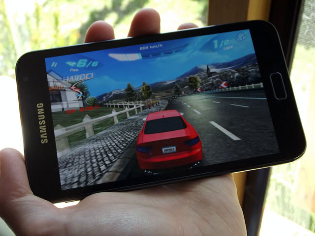
Playing Asphalt 6: Adrenaline on this Galaxy Note would be very difficult without a GPU
Windows Phone is very animation heavy and with the relatively low-power SoCs used in WP devices it would be impossible to get smooth action from simply using the CPU. As such, the GPU plays a big part in rendering the main interface and other animation-heavy UIs, leaving the user with a very smooth experience.
Android is a whole other story. As the original and low-end devices that were available running Android did not have powerful GPUs in them at all it was impossible to offload all 2D rendering tasks to the GPU. Google decided for compatibility reasons that it was better to simply have all rendering done by the CPU (which for early devices wasn’t very good either) and so the signature Android lag was born.
This was corrected finally in Android 4.0 because modern SoCs actually have very capable GPUs, and with old devices almost certainly not getting the update it was time for Google to allow good devices to render the interface elements using their GPU. It is still possible to get a smooth interface from just CPU rendering (as you will see in Android 2.3 devices like the Galaxy S II and Motorola Droid Razr), but the GPU is more efficient so you’ll likely see it getting used for these tasks from here on out.
As you might have guessed, iOS on the iPhone and iPod Touch is very smooth because it renders most interface elements using the GPU. Apple only has to work with a very small selection of hardware and so they can tightly integrate the OS to what is actually available hardware-wise, and so there were minimal problems getting GPU acceleration to work.
Qualcomm Adreno GPUs
The Adreno graphics processing unit is the proprietary graphics chipset used in Qualcomm SoCs. Adreno GPUs used to be called Imageon and they were manufactured by ATI until Qualcomm bought the division from AMD and renamed the products to Adreno. The old Adreno 1xx series were used in old Qualcomm 7xxx SoCs, with the newer Adreno 2xx series being used inside the Snapdragon series.
In the current range of Snapdragon SoCs you see three Adreno 2xx series GPUs used: the Adreno 200 (for S1), 205 (for S2) and 220 (for S3). You might have guessed that a larger number and inclusion in a newer series indicates a more powerful GPU, and you would be correct: Qualcomm states that each successive GPU is twice as fast as the last, meaning the Adreno 220 is around 4x faster than the 200.

Adreno GPUs are used exclusively in Qualcomm Snapdragon SoCs
Adreno GPUs used up to S3 Snapdragons support both OpenGL ES 2.0 and 1.1 along with Direct3D 9.3; Adrenos after and including the Adreno 205 support hardware accelerated SVG and Adobe Flash. These are really all the APIs needed to ensure that modern mobile games work on the smartphone that adopts an Adreno GPU, as no modern games really use the newer OpenGL ES 3.0 API or Direct3D 11 (yet).
In usual Qualcomm fashion there is virtually no information relating to core layout of the Adreno-series GPUs, fillrate statistics or estimated GFLOPS capabilities of these chipsets. This makes it very hard to compare the chips without resorting to a benchmark.
Heading to the future and Qualcomm actually has decided to release information on their chips such as the Adreno 225 which will first appear in their S4 SoCs that use their new Krait core architecture. Unlike the future Adreno 3xx series they do not improve on the API support but do improve on performance: Qualcomm claims they will be 50% faster than the Adreno 220 and roughly on par with the PowerVR SGX543MP2 (found in the Apple A5), capable of 19.2 GFLOPS at 300 MHz.
Imagination Tech PowerVR GPUs
The second major producer of smartphone graphics chipsets is Imagination Technologies, which makes the PowerVR line of mobile GPUs. There have been many series of PowerVR GPUs, though current devices use products from either the PowerVR SGX 5 or 5XT series.
PowerVR GPUs are licensed to other SoC manufactures and so they find their way into a variety of devices. TI OMAP chipsets exclusively use PowerVR GPUs, and you’ll also find them inside some older Samsung Exynos chipsets and also the Apple A4 and A5. They are also sometimes used alongside Intel x86 processors in low-end notebook computers.
The PowerVR SGX 5 series comprises of several GPUs, only a few of which are regularly used. The PowerVR SGX530 is used in the TI OMAP 3 series and so finds its way into a huge array of single-core devices from the Motorola Droid (original) to the Nokia N9. When clocked at 200 MHz, the SGX530 is capable of 1.6 GFLOPS. The SGX535 (used in the iPhone 3GS and iPhone 4) is a die shrinkage of the SGX530 and contains DirectX 9.0c support where the 530 does not, but retains the same performance.

This is a look in to the architecture of the PowerVR SGX 5XT series
The most popular of the 5 series is the PowerVR SGX540 that is used in both the original Samsung Exynos chipset (the Hummingbird) for the Galaxy S along with the TI OMAP 4 series. It has support for DirectX 10 and is capable of 3.6 GFLOPS at 200 MHz, twice that of the SGX530. Unlike the SGX530, the SGX540 can be clocked up to 400 MHz and so theoretically the GPU can achieve 7.2 GFLOPS.
Some people may look at the implementations of the SGX540 and wonder why it appears in the relatively old single-core Hummingbird SoC in the original Galaxy S but also appears in the TI OMAP 4460 dual-core SoC used in the Galaxy Nexus. It turns out the clockspeeds are actually different for both SoCs: the Hummingbird sees the 540 at 200 MHz (delivering 3.2 GFLOPS), the TI OMAP 4430 used in the Droid Razr has it at 304 MHz (~4.8 GFLOPS) and the TI OMAP 4460 at 384 MHz (~6.1 GFLOPS).
The newer 5XT series hasn’t really found its way into many devices yet, with the only notable inclusions being the Apple A5 chip used in the iPad 2 and iPhone 4S and the PlayStation Vita. Where the 5 series only has a single GPU core, the 5XT series supports up to 16 cores, each of which is twice as fast as the SGX540. GPUs in the 5XT are affixed with MPx, where the x denotes the number of cores: for example the SGX543MP2 used in the Apple A5 has two cores.
Currently the SGX543 is the only chip that has found its way into SoCs, with the similar SGX544 scheduled to go into the TI OMAP 5 series. The SGX543 delivers 6.4 GFLOPS per core at 200 MHz, meaning that at the low 200 MHz the SGX543MP2 in the Apple A5 achieves 12.8 GFLOPS which is a considerable improvement over the highest-clocked SGX540. As Apple hasn’t specified what clock speed the GPU in the A5 runs at, my best estimate is around 250-300 MHz based on benchmarks, which means we’re looking at between a whopping 16 and 19 GFLOPS.
I wouldn’t think that too many manufacturers would exceed two cores in the SGX543 as each core added uses more power, but Sony decided that a quad-core SGX543MP4+ is the way to go in the PlayStation Vita. Even if this is clocked at just 200 MHz, the PSVita’s GPU is capable of 25.6 GFLOPS; up that to 300 MHz and you get 38.4 GFLOPS. Like Apple, Sony actually hasn’t specified a GPU clock speed so we can only guess as to how much power the Vita’s GPU actually has.
For interests sake, a PowerVR SGX543MP16 (16-core variant) clocked at the maximum 400 MHz would be capable of 204.8 GFLOPS. That’s enormous and certainly would use a lot of power, but as far as I can tell no such GPU has found its way, or ever will find its way into a production device.
ARM Mali GPUs
The section on Mali GPUs is going to be relatively short because the Mali GPU is currently only used in one SoC: the Samsung Exynos 4210 found in the Samsung Galaxy S II, Galaxy Note and Galaxy Tab 7.7. The Mali range is ARM’s own, so it should be an ideal partner for the Cortex processing cores used in the Exynos chipset.
Even though on paper there are several Mali GPUs, the only one that has really been used is the quad-core Mali-400 MP4 in the Exynos 4210. When ARM says that the Mali-400 MP4 is “quad-core” it is not truly four processing cores like the PowerVR SGX543MP4, it’s simply four pixel shader processors put together. This is why the Mali-400 MP4 does not have the same graphical capabilities as PowerVR’s true quad-core GPU.

This is what's inside a Mali-400 MP4
To quantify the performance the Mali-400 MP4 is capable of 7.2 GFLOPS at 200 MHz, meaning that it is faster than a single-core PowerVR SGX543. The targeted clock speed for use in the Exynos 4210 is 275 MHz, meaning the GPU is capable of 9.9 GFLOPS and making it the fastest GPU available in an Android smartphone at the time of writing.
Roughly speaking the Mali-400 MP4 in the Galaxy S II is twice as fast as the SGX540 in the Droid Razr and ~75% faster than the same GPU in the Galaxy Nexus. In turn, the iPhone 4S’ SGX543MP2 is around twice as fast as the Mali-400 and the Playstation Vita is even faster than that.
Samsung will continue to use the Mali GPUs in their future Exynos 5xxx SoCs, although they will be more powerful units than the Mali-400 MP4. Currently Samsung claims the next Exynos chip’s GPU will be “4x faster” than the implementation in the 4210, but I’d take that with a grain of salt until we find out exactly what is in there.
NVIDIA ULP GeForce GPUs
I mentioned briefly in the processor section of this series that for desktop graphics card manufacturing giant NVIDIA, the GPUs in their smartphone SoCs aren’t particularly impressive. In fact, NVIDIA’s ULP GeForce that is in their Tegra SoCs is the slowest GPU from the first-generation of dual-core processors, and I’ll explain why.
The ULP GeForce is used in two main Tegra 2 chipsets: Tegra 250 AP20H and Tegra 250 T20; the former for smartphones and the latter for tablets. The ULP GeForce used here is clocked at 300 MHz (AP20H) or 333 MHz (T20), and is only capable of 3.2 GFLOPS at 200 MHz. This means that the AP20H at 300 MHz sees 4.8 GFLOPS and the T20 at 333 MHz sees 5.33 GFLOPS.
Now at first glance you would notice that the smartphone GFLOPS capability of the Tegra 2 is the same as the PowerVR SGX540 clocked at 300 MHz, and that is true. However, the maximum clock speed of the SGX540 seen in an actual device is 384 MHz in the Galaxy Nexus, which is capable of 6.1 GFLOPS. This is faster than even the tablet iteration of Tegra 2 at 333 MHz, making the Tegra 2 the least capable GPU.

A Tegra 3 die image, with the GPU hidden inside somewhere
Of course we’re just talking specifics here, and many other factors actually affect the performance of a GPU such as CPU clock speed and display size, but if you’re talking about the most capable GPU the Tegra 2 is definitely not number one.
As we move into the second generation of multi-core processors, NVIDIA was first to strike the market with their quad-core Tegra 3 as I mentioned in my processor article. You would expect that the Tegra 3 ULP GeForce GPU would see a boost, and while it has it might not be as large as you would like.
The Kal-El GeForce is capable of 4.8 GFLOPS at 200 MHz, which you can immediately see is less than the 200 MHz performance of the Mali-400 MP4 and PowerVR SGX543MP2. NVIDIA hasn’t exactly specified what clock speed the GPU is running at in the Tegra 3 chip in devices such as the ASUS Transformer Prime, save for that the clock speed is greater than Tegra 2. If we estimate that it runs at 400 MHz, it’s still only capable of 9.6 GFLOPS which is close to, but just short of the Mali-400 MP4.
Comparison of smartphone GPUs
So now that you know about the different ranges of mobile GPUs available it’s time to see which is the fastest. To do so I’ve made this handy chart that lists them from the most powerful to least in terms of GFLOPS.
Please note that this simply indicates the potential performance of each GPU and does not reflect real-world performance. GPUs are placed in a wide range of systems where external factors such as increased processor clock speeds, RAM types and speeds, display resolutions and more can affect the actual graphical performance of a smartphone.
| GPU | SoC Example | Device Example | GFLOPS at 200 MHz | GFLOPS in SoC |
|---|---|---|---|---|
| PowerVR SGX543MP4+ | PSVita | PlayStation Vita | 25.6 | 25.6+ |
| PowerVR SGX543MP2 | Apple A5 | Apple iPhone 4S | 12.8 |
16 at 250 MHz* |
| Mali-400 MP4 | Exynos 4210 | Samsung Galaxy S II | 7.2 |
9.9 at 275 MHz |
| "Kal-El" GeForce | Tegra 3 | ASUS Transformer Prime | 4.8 |
9.6 at 400 MHz* |
| PowerVR SGX540 | OMAP4460 | Galaxy Nexus | 3.2 |
6.1 at 384 MHz |
| Adreno 220 | MSM8260 | HTC Sensation | N/A | N/A |
| ULP GeForce | Tegra 2 | Motorola Xoom | 3.2 |
5.3 at 333 MHz |
| PowerVR SGX540 | OMAP4430 | Motorola Droid Razr | 3.2 |
4.8 at 304 MHz |
| ULP GeForce | Tegra 2 | LG Optimus 2X | 3.2 |
4.8 at 300 MHz |
| PowerVR SGX540 | Hummingbird | Samsung Galaxy S | 3.2 |
3.2 at 200 MHz |
| Adreno 205 | MSM8255 | HTC Titan | N/A | N/A |
| PowerVR SGX535 | Apple A4 | iPhone 4 | 1.6 |
1.6 at 200 MHz* |
| PowerVR SGX530 | OMAP3630 | Motorola Droid X | 1.6 |
1.6 at 200 MHz |
| Adreno 200 | QSD8250 | HTC HD7 | N/A | N/A |
*these GFLOPS figures are based on estimated (rather than known) SoC clock speeds
Note: Qualcomm Adreno GPUs are included as placeholders in this chart, but as their positions are determined by benchmarks rather than GFLOPS performance there is no way to fully know where they rank
Part 3: Memory & Storage
Again, I hope that you learnt a little bit more with the second part of my series on smartphone hardware. In the next article I’ll be moving through the critical components of a device and landing at memory (as in RAM) and storage types, seeing which is fastest to use and how you can improve your speeds.
If you have any questions about what I have gone over in this guide please feel free to comment below or ask in our forums. I’ll try my best to answer questions but I’m not a hardware manufacturer so I might not have all the answers.
Images courtesy of NVIDIA, Qualcomm, ARM and TI


20 Comments - Add comment