Back in early 2021, we started hearing the first whispers and murmurs of a new kind of cache memory AMD had been working on. The company finally unveiled it later in the middle of the year during Computex, dubbed the 3D V-cache. Essentially, it is the vertically stacked last-level cache (LLC) which allows the company to cram in lots of it in a small footprint.
Currently, AMD is on its 2nd Gen 3D V-cache technology, and recently at CES 2026, it released the Ryzen 7 9850X3D, claimed to be the world"s fastest gaming processor.
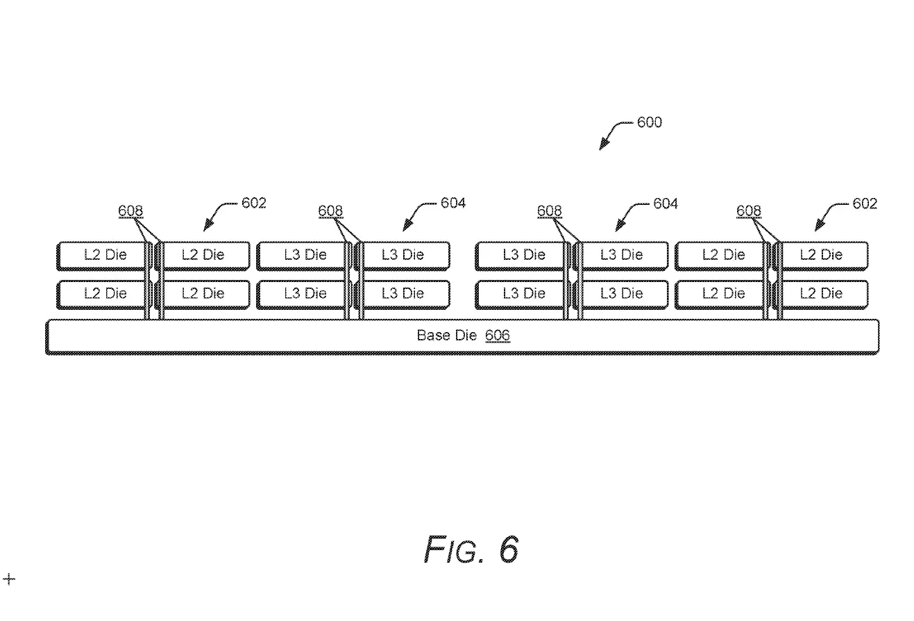
In the case of AMD"s Zen architecture, the last-level cache (LLC) is level 3 (L3), though it looks like the company is now working on making some inroads in its cache hierarchy, as a recent patent suggests AMD is now trying to vertically stack the L2 (level 2) cache as well for even more performance and/or efficiency.
The company has filed a patent for what it calls a “Balanced Latency Stacked Cache,” a design intended to reduce cache memory access delays and improve power efficiency even further in future Ryzen X3D processors.
Compared to 3D V-cache CPUs, conventional planar cached CPUs with no 3D stacked cache have higher latencies and energy costs. This means lower performance and efficiency, respectively. By keeping those benefits in mind, AMD’s new 3D L2 cache memory design claims to reduce the number of cycles required for accessing a typical 1 MB L2 cache memory from 14 cycles down to just 12 cycles.
While this may not seem like a lot, in CPU architecture designing, it is plenty to get excited about, as even shaving off bits like this means a lot for the overall end performance and efficiency. For context, a typical L2 cache has 10-50 cycles, so this is definitely some of the best.
If you are wondering how AMD is making it possible, the patent notes that stacked dies are connected by connection vias like through‑silicon vias (TSVs) or bond pad vias (BPVs) for vertical silicon-to-silicon communication, and these connection vias are routed through the center, thus shortening the wire stages or pipe stages. Also, by routing the via connections through the center of the stacked dies, AMD creates a symmetrical or balanced structure that should help ensure that data access times are uniform across all layers. This is also why the patent is called "Balanced Latency Stacked cache".
The patent is still pending so it remains to be seen what happens. Of course just because it is being filed does not mean it will come to the market. There can be a lot of difference between a theoretical expectation and the real-world performance.
Via: Google patents (US20260003794A1)