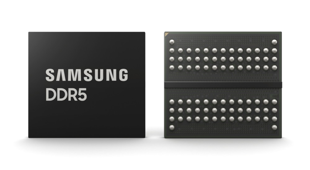
Samsung Electronics has announced that it has started mass production of the industry's smallest, 14-nanometer (nm), DRAM based on extreme ultraviolet (EUV) technology. The tech giant has increased the number of EUV layers to five to provide a leading DRAM process for its DDR5 solutions, succeeding Samsung's shipment of the industry-first EUV DRAM in March of 2020.
Senior Vice President and Head of DRAM Product & Technology, Jooyoung Lee stated:
We have led the DRAM market for nearly three decades by pioneering key patterning technology innovations. Today, Samsung is setting another technology milestone with multi-layer EUV that has enabled extreme miniaturization at 14nm — a feat not possible with the conventional argon fluoride (ArF) process. Building on this advancement, we will continue to provide the most differentiated memory solutions by fully addressing the need for greater performance and capacity in the data-driven world of 5G, AI and the metaverse.
EUV technology has become more and more essential to enhance patterning accuracy for greater yields and higher performance as DRAM goes on to scale down the 10nm-range. The company has been able to achieve the highest bit density while boosting the overall wafer productivity by more or less 20 percent by applying five EUV layers to its 14nm DRAM. Furthermore, the 14nm process, as compared to the previous-generation DRAM node, is also capable of aiding in bringing down power consumption by roughly 20 percent.

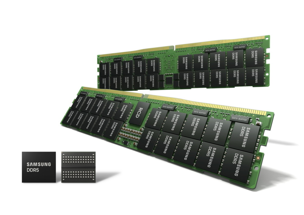
Samsung's 14nm DRAM will aid in achieving unprecedented speeds of up to 7.2 gigabits per second (Gbps), leveraging the latest DDR5 standard. The speed of 7.2Gbps is more than twice the DDR4 speed of up to 3.2Gbps. The tech giant intends to broaden its 14nm DDR5 portfolio to support data center, supercomputer, and enterprise server applications. Samsung also has plans of expanding its 14nm DDR5 chip density to 24Gb to meet the data demands of global IT systems.